SCIENCE & TECH.
The Wall Every Chipmaker Is Racing Toward
For seventy years, the entire computing industry has run on a quiet promise: chips get smaller, faster, and cheaper roughly every two years, a rule of thumb known as Moore's Law. It's the reason the smartphone in your pocket has more computing power than the room-sized machines that sent astronauts to the Moon. But that promise has always come with a ticking clock, because you can only shrink a piece of silicon so far before the laws of physics start fighting back.
That fight is now happening at a scale almost too small to picture. Modern top-tier chips, like the ones Taiwan Semiconductor Manufacturing Company (TSMC) began mass-producing on its 2-nanometer-class "N2" process late last year, pack transistor features into spaces just a few atoms wide. Squeeze silicon much thinner than that, and it stops behaving like a reliable on-off switch. Electrons start leaking where they shouldn't, defects at the material's surface scatter the current, and the whole point of a transistor — cleanly switching between "on" and "off" — starts to break down. Samsung is chasing a 1.4-nanometer node for 2027; Intel is racing to get its 18A process to "world-class" yields by the same year. Everyone in the industry is converging on the same uncomfortable conclusion: pure silicon is running out of road.
Enter the One-Atom-Thick Material That Wouldn't Cooperate
For more than a decade, researchers have eyed a category of materials called two-dimensional, or 2D, semiconductors as the most promising way to leapfrog silicon's limits. The star of the show is molybdenum disulfide, or MoS2 — a material that can be grown just one atom thick while still conducting electricity in a controllable way. In theory, a transistor built from a single atomic layer of MoS2 could be smaller, faster, and dramatically more energy-efficient than anything silicon can achieve.
In practice, MoS2 has fought back. Every transistor needs a paper-thin insulating layer called a gate dielectric sitting on top of the semiconductor, acting like a traffic cop that controls the flow of electrons through the device. Make that layer thinner and you get tighter, more precise control — which is exactly what chipmakers want as transistors shrink. But MoS2's surface has no "dangling bonds," the loose chemical hooks that other materials use to grab onto a new layer being deposited on top of them. Try to grow a dielectric material directly onto MoS2 using standard techniques, and the result is uneven, full of microscopic gaps and defects, and electrically messy — killing exactly the performance gains researchers were chasing in the first place. For years, engineers were stuck picking one of two options: tighter electrical control, or better electron flow. Nobody could get both at once.
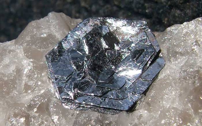
Molybdenum disulfide, or MoS2
A Buffer Less Than Half a Nanometer Thick
That's the problem a team led by Professor Wen-Hao Chang and Professor Tsung-En Lee at NYCU, working with TSMC Corporate Research under Dr. Iuliana Radu, says it has cracked — and their solution, published this month in the journal Nature Electronics, is almost absurdly small.
Rather than hunting for an entirely new semiconductor material, the team focused on the narrow, awkward no-man's-land where two materials meet. They deposited an ultrathin layer of aluminum directly onto a single atomic layer of MoS2, then carefully oxidized it, producing a layer of aluminum oxide roughly 0.42 nanometers thick — for context, that's smaller than the width of a single water molecule, and about one five-hundred-thousandth the width of a human hair. Only after laying down that whisper-thin buffer did the team add the thicker, high-performance hafnium oxide layer that does the heavy lifting as the transistor's actual gate dielectric.
"For many years, efforts to improve atomically thin transistors have largely focused on discovering better semiconductor materials," said Professor Chang, the study's corresponding author. "Our research shows that the atomic interface between materials can be just as important. By engineering that boundary, we were able to reduce one of the fundamental trade-offs that has limited two-dimensional transistors for many years."
The tiny aluminum oxide layer does two jobs at once. First, it gives the hafnium oxide gate dielectric a smooth, continuous, defect-free surface to grow on, instead of the patchy, gap-riddled mess that forms when it's deposited directly onto bare MoS2. Second, it acts as an electrical shock absorber, damping down unwanted interactions between the dielectric and the semiconductor that would otherwise scatter electrons and slow the whole device down.
The Numbers That Have Chip Engineers Paying Attention
Numbers in materials science can be dry, but these ones matter. Using the new interface, the NYCU-TSMC team built short-channel transistors with an equivalent oxide thickness of around one nanometer — essentially matching the electrical thinness of the industry's best silicon dielectrics, but on a material only one atom thick underneath. The devices showed low leakage current (meaning less wasted power and heat), minimal hysteresis (meaning the transistor behaves predictably rather than "remembering" its last state in unwanted ways), and a maximum transconductance of 0.45 milliSiemens per micrometer in transistors with 100-nanometer channels — a measure of how efficiently the device amplifies an electrical signal, and a genuinely strong result for a 2D transistor.
Crucially, the team didn't build these devices from painstakingly hand-assembled flakes of MoS2 peeled off with tape, the way many lab demonstrations of 2D materials are made. They used chemical vapor deposition (CVD) to grow the MoS2 across a larger area, a process much closer to what an actual chip factory would need for mass production. That detail is what turns this from a nice physics result into something TSMC's research arm considers worth co-authoring.
Why the World's Biggest Chipmaker Is in the Room
TSMC's involvement is the tell here. The company isn't in the habit of putting its name on speculative academic curiosities — it manufactures the vast majority of the world's most advanced chips, for customers including Apple, Nvidia, and AMD, and its research priorities tend to map closely onto what it actually expects to need in its factories over the coming decade. The International Roadmap for Devices and Systems, an industry-wide technology forecast, has listed 2D semiconductors as the leading candidate to eventually replace silicon channels since 2018, and organizations including Belgium's imec, along with TSMC and Intel, have been quietly building out 2D-material research programs for years.
That said, nobody in the industry is expecting phones with atom-thin chips next Christmas. Some of the more detailed industry roadmaps circulating this year peg a full transition to 2D-semiconductor channels as roughly a decade-plus away, likely closer to the early 2030s at the earliest for niche applications and the following decade for anything mainstream. What this research does is remove one specific, long-standing engineering obstacle from that timeline — not eliminate the timeline itself. As Professor Tsung-En Lee put it: "When transistor components become only a few atomic layers thick, the interface is no longer simply the boundary between materials, it becomes an active part of the device. Learning to engineer these interfaces with atomic precision opens new opportunities for designing future semiconductor devices that would be difficult to achieve by changing individual materials alone."
Expert Perspective
Materials scientists outside the project have noted that the significance here lies less in any single number and more in the shift in strategy it represents. For much of the last decade, the hunt for silicon's successor has centered on finding a better semiconductor material — a new element or compound that simply outperforms silicon on its own merits. This work suggests that the interfaces between materials, the literally atom-thin seams where one substance ends and another begins, may end up mattering just as much as the materials themselves. As transistor components shrink toward the size of individual atoms, there is proportionally less "bulk" material and proportionally more surface and interface — meaning the boundary effectively becomes the device, rather than just a detail around its edges.
That reframing has ripple effects beyond this one result. If interface engineering, rather than material discovery alone, is the more productive lever to pull, it opens the door for many more incremental, atom-by-atom improvements from labs and companies that don't have to invent a wholly new material to make progress — a lower bar that could speed up the whole field's pace of advancement.
What This Means for You
It's easy to read "0.42-nanometer aluminum oxide layer" and assume this has nothing to do with your life. In the long run, it very much does. Every leap in transistor efficiency eventually shows up as a longer-lasting phone battery, a laptop that doesn't get hot on your lap, a data center that can run the same AI model on less electricity, or a self-driving car's onboard computer that can process more sensor data without cooking itself. The current AI boom is straining chip supply chains and power grids simultaneously; any credible path to transistors that do more work per watt is, in a very real sense, a partial answer to both problems at once.
The honest caveat is timing. This is a laboratory result, not a shipping product, and the researchers themselves say more work is needed before the fabrication process can be scaled up for mass manufacturing. Don't expect "2D chip" branding on next year's flagship phone. But when the world's largest chip manufacturer co-authors a paper solving a problem the whole industry has been stuck on, it's a meaningful signal about where engineering resources — and eventually, products — are headed.
Conclusion
Silicon isn't dead yet, and it won't be for years. TSMC, Samsung, and Intel are all still racing each other down the silicon roadmap toward 1.4-nanometer chips and beyond, squeezing out the last available gains from a material that has defined computing since the 1960s. But this month's breakthrough is a reminder that the industry's contingency plan for when silicon finally does run out of road just got noticeably more real — built not from a brand-new wonder material, but from a smarter idea about the almost-nothing space where two materials meet.
Published By | Tech Wiz